
ADVANCED PRECISION PROCESSING

APPLICATIONS

ADVANCED PRECISION PROCESSING

Explore specialized plasma approaches for precision manufacturing and advanced material applications.

WHAT IS PRECISION PLASMA PROCESSING?

Some applications require plasma processes that go beyond standard surface treatment — micrometer-scale patterning, highly controlled etching, or processing under tight tolerances for demanding manufacturing environments such as semiconductors and advanced electronics. These applications typically call for low-pressure plasma systems with precise process control over gas composition, power and exposure time.

How it Works

Precision plasma processes rely on tightly controlled vacuum environments, where gas composition, pressure, power and exposure time are precisely managed to achieve repeatable, micrometer-scale results. This level of control supports applications where even small process variations can affect performance or yield.
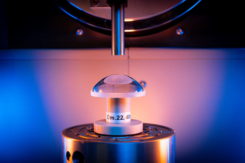
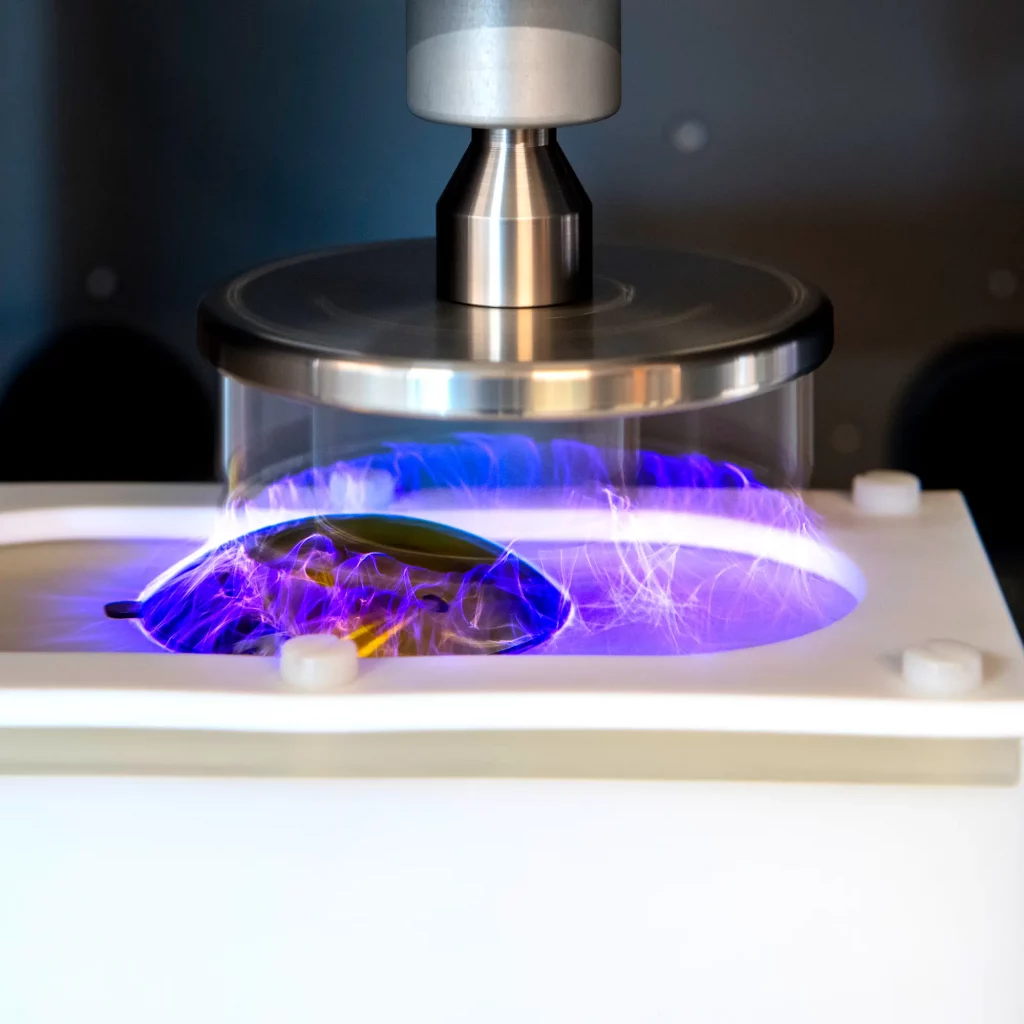
satisloh spp 200 center thickness measuring dsc08999
tantec 37

TYPICAL APPLICATIONS

Semiconductor and electronics component processing
Micro-scale device manufacturing
Precision biomedical device components
Custom research and development applications
Selective surface treatment for masked or patterned applications

KEY BENEFITS

Tight Tolerances

Suited to micrometer-scale precision requirements.

High Repeatability

Controlled vacuum environment supports consistent, repeatable results.

Custom-Engineered

Processes developed around your specific precision and material requirements.

Want to go deeper? Read: Atmospheric vs. Low-Pressure Plasma

NEED PRECISION PLASMA PROCESSING?

Tell us about your tolerance, material and precision requirements.

Scroll to Top