
Electronics manufacturing places some of the tightest demands on surface preparation of any industry — components are small, tolerances are tight, and materials are often sensitive to heat, moisture and chemical exposure. Plasma technology has become a standard tool for meeting these requirements without compromising the underlying components.
Common Uses in Electronics
- Cleaning circuit boards before wire bonding or encapsulation
- Surface activation ahead of underfill or encapsulant dispensing
- Preparing flexible substrates for printed or flexible electronics
- Removing oxidation and contamination from contact surfaces
Why Precision Matters Here
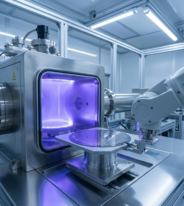
In electronics applications, even microscopic contamination or an improperly wetted surface can cause a bonding or encapsulation failure that only shows up later, during reliability testing or in the field. Plasma processes used in this space typically require a high degree of process control and repeatability — which is why low-pressure plasma systems are common in this industry, alongside atmospheric solutions for higher-throughput steps.
Looking Ahead
As electronics continue to move toward smaller form factors, flexible and printed formats, and new material combinations, plasma processes are likely to play an even larger role in enabling those manufacturing approaches.